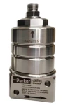
铱涂层钛 PTL - 针对 PEM 电解进行了优化


- 铱涂层电极,针对 PEM 水电解(阳极侧)进行了优化
- 纳米多孔铱层通过压入辅助 火花烧蚀法应用,不含粘合剂,超均匀
- 高孔隙率钛多孔传输层
- 有多种尺寸可供选择:1x1 cm 到 15x15 cm(可定制切割)
- 专为苛刻的 OER 条件而设计,具有高耐用性和导电性
- 适用于 CO₂RR、N₂RR、 高电流密度设置等
- 铱负载选项 从 0.1 mg/cm² 到 1 mg/cm²
- 还提供涂层服务 - 将您自己的 PTL 发送给我们
。
AI 生成的翻译
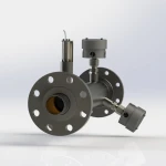
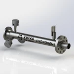
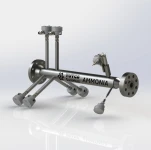
铱涂层钛 PTL - 专为 PEM 电解而优化
我们的铱涂层钛 PTL 专为高性能 PEM 电解槽而设计,它将高孔隙率基底与无粘合剂、超均匀的铱催化剂层相结合。我们采用专有的冲击辅助火花烧蚀技术,可提供耐用、纳米结构和可扩展的涂层。这样就形成了一个高度稳定的电极平台,适用于工业电解和高级电化学研究。
主要特性
-
使用火花烧蚀法进行均匀的铱涂层 - 无粘合剂、无溶剂
-
纳米结构催化剂层可实现最大表面积和活性
-
高孔隙率钛 PTL 基底(30-80%),来自莫特、贝卡尔特或恒科、贝卡尔特或 Hengko 的高孔隙率钛 PTL 基底(30-80%)
-
在 OER 环境中具有出色的耐腐蚀性
-
与大多数 PEM MEA 堆和测试装置完全兼容
-
工作温度范围:室温至 120°C
应用 &;使用案例
-
PEM 水电解(阳极侧) - 实验室规模和工业电流密度
-
高电流密度系统 - 包括 CO₂RR 和 N₂RR 设置
-
定制电化学 R&;研发--灵活的尺寸和铱载荷非常重要
-
MEA 原型开发& 基准测试--催化剂层研究的理想选择
-
堆栈组件集成--商业电解槽设计工作流程
规格
-
基底: 钛多孔传输层 (PTL)
-
涂层材料: 铱
-
涂层方法: 嵌入式辅助火花烧蚀
-
电极厚度: 250 µm ± 5 µm
-
孔隙率: 30% 至 80%
-
操作温度: RT 至 120°C
-
标准尺寸: 1x1 cm、2x2 cm、2.5x2.5 cm、3x3 cm、5x5 cm、10x10 cm、15x15 cm
-
铱负载: 0.1 mg/cm² 至 1.0 mg/cm²
-
兼容性: PEM 电解器、CO₂RR、N₂RR 和类似的先进电化学系统
-
供应商: VSParticle B.V.、荷兰
定制选项
-
定制铱载量:从低(0.1 mg/cm²)到高(1.0 mg/cm²)
-
纸张尺寸:我们提供非标准格式的裁剪(例如、2.2×2.2 厘米),不收取额外费用
-
涂层服务:将您自己的钛 PTL 发送给我们,我们将为您涂上铱涂层
-
使用我们的火花烧蚀技术,保证批次间的一致性
。
| 品牌 | VSParticle |
| 品牌 | VSParticle |
| 最高环境温度(°C) | 120 |
VSParticle
AI 生成的翻译
VSParticle is a deep-tech company redefining how advanced materials are developed and manufactured. Originating from research at Delft University of Technology, VSParticle enables precise, dry, and scalable production of nanoporous layers using a proprietary spark ablation technology.
We empower scientists and engineers to rapidly prototype and scale high-performance materials, especially for applications in green hydrogen, electrocatalysis, sensing and semiconductor fabrication.
With a strong foundation in nanotechnology and material science, VSParticle offers the full solution in nanomaterial development. Our Nanoparticle Generator provides clean and controlled nanoparticle production, while our NanoPrinter, allows direct and precise deposition to create nanoporous layers.
These support the production of advanced electrodes such as iridium-coated Porous Transport Layers (PTLs), engineered for optimal performance in PEM water electrolysis, that is maintained at low iridium loadings. Our coatings are ultra-pure, binder-free, and tunable to specific performance needs, offering unmatched flexibility for research labs and industrial partners alike.
VSParticle’s systems and materials are used globally by innovation leaders working to accelerate the energy transition and develop the next generation of electrochemical devices.
最新产品

浏览 Hyfindr 数字生态系统

Hyfindr
B2B 供应商

Hyfindr
技术 视频

Hyfindr
技术 知识

Hyfindr
技术 咨询

Hyfindr
技术 社区